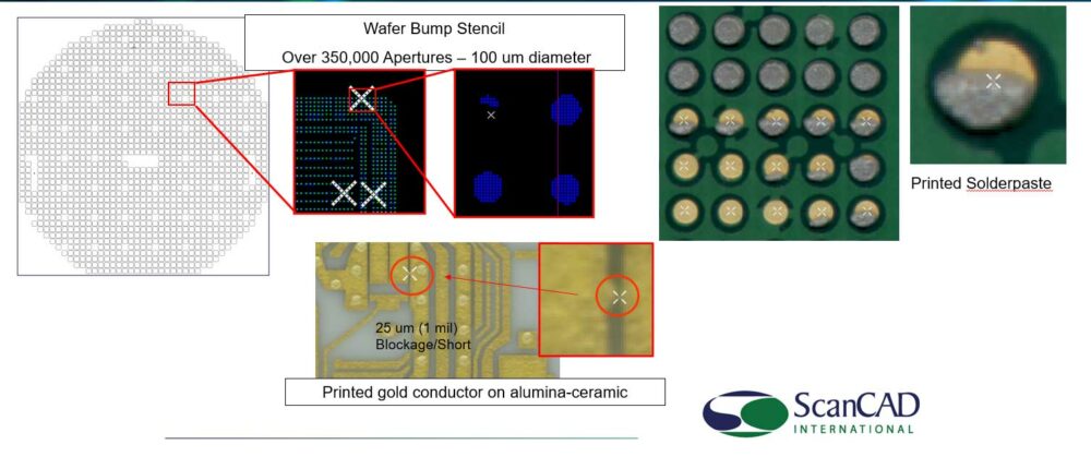
Solder paste stencils are essential tools for PCB manufacturing, as they allow precise and consistent application of solder paste to the pads of surface-mounted components. However, solder paste stencils are also prone to various defects that can affect the quality and reliability of the solder joints. Some of the common defects and their causes are listed below:
- Missing Apertures: While uncommon, there are certain circumstances where an aperture can be entirely missing from a stencil. This will cause a complete lack of solder on the correlating pad.
- Extra Aperture/Pinhole: This tends to be more common in electroformed stencils; this defect occurs when there is a small opening in an area of the stencil where no opening should be present. This can lead to solder being applied to the circuit board where none should be present and can lead to electrical shorts or other issues.
- Undersized or Clogged Apertures: This occurs when the stencil apertures are not cut to the correct size, clogged or damaged. This results in insufficient or uneven solder paste deposition on the pads.
- Oversized Apertures: This occurs when the aperture openings are too large for the pad and results in too much solder being printed. This can lead to bridging or potential shorts even after passing electrical testing.
- Stretch: Over time, the stencil itself can become stretched and warped leading to misalignment relative to a given PCB. This defect is generally not present at the time of manufacture and increases slowly during use.
- Misalignment: There are several potential causes for misalignment including poor stencil fabrication or even poor PCB fabrication. There are numerous causes leading to the stencil not properly aligning with the PCB. In all cases, misalignment can lead to a variety of solder defects including bridging, too much solder, too little solder, etc.
These defects can occur at various times during their lifecycle meaning that continued inspection and validation of a solder paste stencil over its lifecycle is critical to avoiding expensive solder paste defects. The ScanCAD ScanSTENCIL automatic inspection system is a powerful and innovative solution for detecting and preventing solder paste stencil defects and can be used by both stencil users and stencil fabricators. The system uses a high-resolution optical scanner and advanced image processing techniques to capture and analyze images of stencils and their respective PCBs. The system can automatically identify and measure all of the defects listed above helping stencil fabricators assure quality of their product while also providing stencil users valuable insight into the performance of their stencils over time.
ScanCAD supports numerous stencil users and fabricators throughout the world today and helps to ensure continued quality and customer satisfaction at the time of manufacture. Simply confirming a stencil meets the quality standard upon fabrication however, is not enough to avoid defects in the future. ScanCAD has recently been collaborating with numerous stencil users (contract manufacturers and other assembly firms) to help manage the complete stencil lifecycle including:
- Incoming Validation: Users will validate that the incoming stencil meets or exceeds their requirements upon receipt. Even though most suppliers are already inspecting their stencils, defects can occur in ways that may not be captured, i.e., a defect may be introduced when the CAD data is stepped and repeated. The ScanCAD system is capable of inspecting against the stencil cut file OR the original CAD data! The ScanSTENCIL system is NIST traceable and provides the necessary validation that the incoming stencil conforms to specified quality requirements; a critical feature for any ISO9001 or AS9000 certified firm.
- Cleaning: Users can confirm that each and every aperture opening on all stencils are properly cleaned and avoid costly defects caused by dirty stencils.
- Degradation: Each inspection performed after cleaning will also inspect for stencil degradation including stretch and wear on individual apertures. Users can construct a deep understanding of the lifecycle of their stencils over time and make educated decisions on when to retire and replace a given stencil.
Managing the overall lifecycle of a stencil, from fabrication, to validation, and periodic inspection is critical to avoiding costly solder defects. The ScanCAD ScanSTENCIL system is perfectly suited to support firms in inspecting and validating solder paste stencils during every stage of its lifecycle. It is flexible, powerful, and NIST traceable, supporting AS9000 and ISO9001 certifications.
Examples of Defects found by Automatic Inspection


