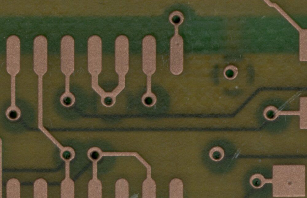
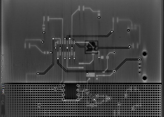
PCB Reverse Engineering is the generation of circuit board design data to replicate or re-create an existing product. PCB Reverse Engineering is a discipline that is the equivalent of an analytical multi-tool, with the ability to completely recreate design data for a product from scratch. Reverse engineering capacity is a healthy marker for any mature industry and a critical component in ensuring system continuity for everything from consumer electronics to aerospace and defense to medical, automotive and telecommunications.

When PCBs are initially designed, they are created by a designer who stores the design on some sort of storage medium. Historically, mylar films were used to both store and produce PCBs, but modern techniques have moved away from this method. Regardless of the method used, no factory or location is completely impervious to natural disaster or human error, and designs can become lost or damaged over a product’s lifespan. The loss of original design data for a PCB represents a loss in the ability to control a product’s design and to reproduce the product.
PCB Reverse engineering can also be used to fill in partial data gaps in a circuit assembly data package. For example, if you only have a bill of materials and a physical PCB, ScanCAD can use the board to generate the bare board design data and a schematic.
ScanCAD uses two main methods of reverse engineering PCBs. The first method is a proprietary milling and imaging process that captures high resolution, NIST-calibrated images of each circuit layer on the PCB. The vector or Gerber data is then reconstructed using these images. The gerber data generated in this process serves as the backbone for the rest of the project, allowing us to generate component Pick and Place/Centroid Data, Netlist and Schematic data. This process yields exact copper geometries and identically matches the original PCB’s form, fit and function down to the mil — for every single layer, even inner layers.
The second way we reverse engineer PCBs is a non-destructive method involving the use of Flying Probe Test (FPT) machines for connectivity-only reverse engineering. In this method, the PCB must be depopulated (and loses its functionality) but the bare board is not destroyed. Additionally this method does not allow us to capture inner copper geometries.

Our primary outputs include:
- Bare Board Fabrication Data (Gerber RS274x, Excellon II Drill, ODB++, IPC-2581)
- Component and Assembly Data (ASCII Pick and Place/Component Centroid, IPC Netlist)
- Supporting Documentation (Bill of Materials, Schematic)
This is not an exhaustive list, so if there’s something you’d like us to generate data for that you don’t see here, feel free to ask!
News
Introducing the ScanCAD Software Assistant: Instant Answers, Anytime
We’re excited to announce a new addition to the ScanCAD support experience — the ScanCAD Software Assistant, now available within the customer portal on our website for all active warranty...
Celebrating Jeff Rupert and his role at ScanCAD
We are celebrating Jeff Rupert and his powerful role in shaping ScanCAD and what it is today, as well as where we are going as a company tomorrow. Jeff is stepping back from his full-time role into...
ScanCAD donates SMT system to Universidad Autónoma de Ciudad Juárez
Giving back is at the very core of what we believe to be important in our business. We always love to hear about the outcome following a donation or involvement and wanted to share a story from our...
Holiday Wishes 2025
Season's GreetingsTo the entire ScanCAD International global community, our friends, family, customers, representatives, and distributors. Thank you, sincerely, for another year — it is an honor and...
Honoring Our Legacy, Writing Our Next Chapter
It is with a profound sense of purpose and gratitude that I announce I will be transitioning from CTO to CEO of ScanCAD International, effective January 1, 2026. This moment is not a sudden shift,...
Is Your Manufacturing Process Ready for the Future of Electronics?
Is Your Manufacturing Process Ready for the Future of Electronics? The electronics manufacturing industry is facing a perfect storm of shrinking device sizes, increasing performance demands, and...
Trade shows
ScanCAD participates in many trade shows during the year, whether in ScanCAD's booth or by way of our distributor/OEM.
IPC APEX 2026
Anaheim, CA USA
March 17-19, 2026
ScanCAD Booth #3407
DMC 2026
Orlando, FL, USA
March 28 - April 2
ScanCAD Booth #128

