
Process Control
Request More InformationThe apparently simple operation of placing components on a circuit board is far more delicate than it seems. This single operation actually requires a careful balance between manufacturing tolerances/accuracy of a variety of different systems. First, the solder paste stencil (usually sourced externally) is produced from a master dataset. Solder paste stencil fabrication is a fairly accurate process, however like anything, is subject to the real world, and thus manufacturing tolerances. The resultant stencil will inevitably vary from the master dataset. Second, a batch of boards is fabricated. PCB fabrication tends to be far less accurate and results in a job lot of circuit boards that are generally consistent internally, but are subject to significant deviation from the original design. The stencil and the board are brought together and paste is deposited on the board. Lastly, components are placed on the circuit board, again using coordinate locations supplied by the master dataset.
In theory everything comes together beautifully at this point and there are no errors!
In reality the additive differences from the stencil, the board, and the component placement machine overcome the tolerance of the process, and defects are introduced. Defects are generally seen on the smallest pitch devices where the tolerance is the tightest and they are generally randomly distributed. It can be a nightmare trying to track down and minimize or eliminate these defects because there is no single failure point. Component placement machine operators may spend hours simply adjusting offsets in order to get the boards to run. There must be a better way!
Good news, there is a better way!
Address the Root Cause
The root cause is not a failure in any one of the elements coming together. More than likely, the stencil is manufactured within specification, the board is manufactured within specification, and the component placement machines are calibrated and operating within specification. The problem is the cumulative tolerance deviation that occurs when all three of these independent processes come together on the production line violating what is required for error-free placement. The window of alignment for all three elements could be too small to operate within.
Instead of fighting with offsets and trying to force an overtaxed system to operate – address the root cause!
The root cause is that the stencil, the board, and the component placement machine are all compounding tolerances together at the time of solder paste printing and component placement.
Defects at this stage are expensive, difficult to understand, and unnecessary.
Improve your Process
Instead of using the same master dataset for all three stages, follow a more modern approach. Use the master dataset in order to manufacture the job lot of circuit boards. Then, use our systems to modify the stencil and component data to match the job lot of PCB’s exactly. In effect, the tolerances are no longer compounded and errors in solder paste deposition and component placement are reduced dramatically. Furthermore, our process allows potential issues with either the stencil, or the board, to be detected upstream and before value is added and material wasted.
Reduce defects, save operator time, and increase yield.
Unique Technology
Internally developed software coupled with our low-cost vision platform and NIST certified calibration equipment ensures that our system is a solution that is custom tailored to help you improve your processes and give you the visibility and insight you need. Our proven hardware and software have been specifically designed to maintain an excellent price-performance ratio, maximize your ROI and provide a unique set of tools for effective and efficient process improvement.
100% traceability and SPC data for your quality certification and compliance requirements.
Case Studies
Motorola published a study in SMT Magazine focusing just on adjusting the stencil data to match the PCB. This study was limited to the stencil data only, the component placement coordinates remained altered. Even so, Motorola documented a 43% reduction in solder paste defects. The study was conducted on 125,000 parts. The scatter chart on the left below indicates the deviation when using the original data while the chart on the right depicts the results gained from simply altering the stencil cut data to match the job lot of PCB’s.
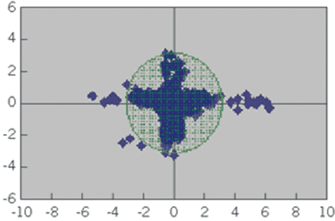
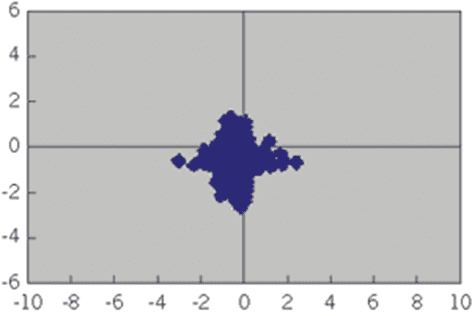
If a 43% reduction in solder paste defects can be achieved by altering the stencil data alone, imagine the improvement made possible by conforming both the stencil and the component placement file to the board!
In a separate study conducted in partnership with a ScanCAD contract manufacturing customer, both the stencil and component placement data were modified to match the job lot of PCB’s. The conformed data led to a greater than 60% reduction in 0201 and 0402 tombstoning and significantly increased visibility into other variables impacting performance. The insight gained allowed the customer to further tighten and improve other areas of the process that had been masked by compounded tolerances.
Properly conformed data and increased visibility leads to greater than 60% reduction in tombstoning and significant insight into process improvement!
Technical Specifications*
Scanner
- High-Resolution Color Flatbed Scanner, Size A3:(400/1000/1600/2000/2400/3200/4000/ 4800 dpi) Calibrated Accuracy: ± 0.001” (± 0.0254mm)
- A3-Scanning Bed Area: 11.7″ x 16.5″ (297mm x 419mm)
- Multiple scans can be stitched together for a larger working area
Computer**
- Multi Core Processor – 3GHz
- 1TB 7200 RPM HD, 8-16 GB RAM (Additional 256 GB SSD recommended for higher performance)
- FHD (1920X1080) Flat Panel Monitor
- Ethernet Connection
- Windows 10 – 64-Bit
- 2 available USB ports – USB2 or USB3
**Recommended customer-supplied minimum PC requirements.
Additional System Components
- Precision Glass NIST Calibration Grid
- Software Protection Key
- Custom Transmissive Lighting Package
- Custom Workstation Desk
- Scanning Accessory Package
The following are trademarks of the indicated companies: Gerber, Ucamco N.V.; Windows 10, Microsoft®; ScanCAD™ and ScanINSPECT VPI™ are trademarks of ScanCAD International, Inc. *All specifications and designs subject to change without notice.*
Datasheets
News
Give us your Feedback, please
We would love to hear from you! What products, features and services would you like to see? Now is your chance to give us your wishlist!
Fully Editable Native Board Layouts, Direct From Reverse Engineering
Fully Editable Native Board Layouts, Direct from Reverse Engineering Reverse engineering recovers what's lost. Now it delivers what's next. For over 30 years, ScanCAD International's...
Introducing the ScanCAD Software Assistant: Instant Answers, Anytime
We’re excited to announce a new addition to the ScanCAD support experience — the ScanCAD Software Assistant, now available within the customer portal on our website for all active warranty...
Celebrating Jeff Rupert and his role at ScanCAD
We are celebrating Jeff Rupert and his powerful role in shaping ScanCAD and what it is today, as well as where we are going as a company tomorrow. Jeff is stepping back from his full-time role into...
ScanCAD donates SMT system to Universidad Autónoma de Ciudad Juárez
Giving back is at the very core of what we believe to be important in our business. We always love to hear about the outcome following a donation or involvement and wanted to share a story from our...
Holiday Wishes 2025
Season's GreetingsTo the entire ScanCAD International global community, our friends, family, customers, representatives, and distributors. Thank you, sincerely, for another year — it is an honor and...
Trade shows
ScanCAD participates in many trade shows during the year, whether in ScanCAD's booth or by way of our distributor/OEM.
IPC APEX 2026
Anaheim, CA USA
March 17-19, 2026
ScanCAD Booth #3407
DMC 2026
Orlando, FL, USA
March 28 - April 2
ScanCAD Booth #128