
In this modern age, technological advancements in manufacturing continue to roll forward at an ever increasing pace.
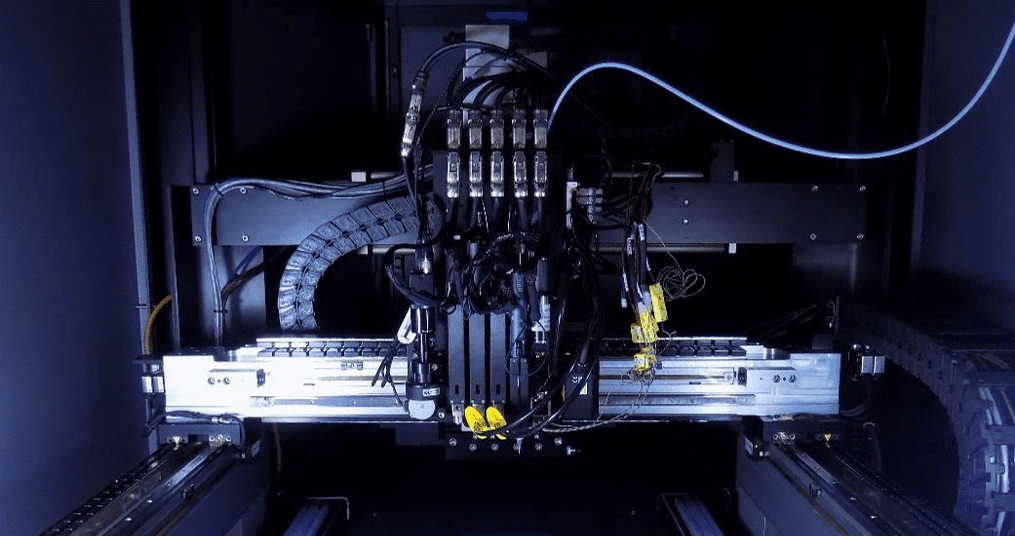
The picture above shows a multi-material, 3-D, Fused Deposition Modeling (FDM) printer that is capable of printing circuit boards – from scratch! Normally, a PCB starts as a series of fiberglass and resin pieces, and copper “foil” layers are laid across or grown out onto these base substrates creating copper-clad plates. These plates are then coated with photo resistive coating and exposed to an image of a circuit. All areas that are NOT part of the circuit are then removed using a chemical etching process. Once each of the different layers are completed, they are all pressed together to make a single PCB using high temperatures and extreme pressure to bind the layers of the board together. Finally the resulting bare board is drilled, sometimes in multiple iterations, in order to establish electrical connections between the different layers. This process is expensive, requires many different processes, machines, and even chemistry.
This has been the way PCBs have been fabricated for decades – sure, tech has improved vastly upon the manner in which the fabrication occurs but the process is basically the same for much of the PCB fabrication industry today.
Enter the dawn of additive manufacturing and the 3D printer.
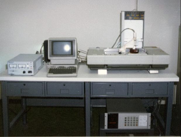
Ok ok, you won’t be able to pick up one of these machines on Amazon. The image above is a photo of the very first additive manufacturing device, an SLA (stereolithography apparatus). It was developed in 1983 and released in 1987, the 3D Systems’ SLA-1 was the first 3D printer to become commercially available. In 1989, the most commonly used method of printing (Fused Deposition Modeling, or FDM) was patented. And, when the patent for FDM expired in 2009, the consumer market was open for business, starting with Makerbot Kickstarter project. Thus began the recent renaissance in additive manufacturing and 3D printing.
Fast forward to 2019 – ScanCAD and nScrypt have taken a long look at the technology involved in 3D printing and realized – we don’t need a whole factory to produce circuit boards. Boards can be imaged, reverse engineered, and reproduced in single/small batch with turnaround times in hours instead of months. And, on top of that, you will be using small equipment and handful of supplies that will all fit in the trunk of your car, or in a storage hatch in a space shuttle, or in small self-contained structure deployed to service damaged military equipment in the field (you get the picture). Now, we can have replacement parts printed at our fingertips, ready for implementation into whatever equipment is in need, where ever it is needed. In addition, once a part has been re-engineered for FDM printing, you will be able to print as many of them as you have the raw supplies for.
So how does it work?
While the concept behind the final PCBA/CCA (PCB Assembly or Circuit Card Assembly) remains the same, the way that we get there has changed. Instead of using flat sheets of dielectric and copper foil, heat, chemicals and massive presses, an FDM type printer is able to take advantage of different types of filaments to produce the various conductive and non-conductive portions of the PCB. In the first image above, the machine has been set up with 5 individual printing/extrusion heads, which allow for the printing of – you guessed it – 5 different types of filaments.
These filaments can vary in size and makeup in order to allow the machine to quickly produce the various aspects of a PCB, from conductive traces and vias to the board’s substrate to silkscreen, as well as adhesives or solderpaste for components. Once the gerber data is generated for the board, it is given to the 3-D Printer’s software for slicing (the process of taking a 3-D data cloud and turning it into individual 2-D slices/layers to be printed) and the printer prints the physical board. Instead of pressing materials together and drilling out the layer-to-layer interconnects, the vias that run between the conductive layers will be printed along with the layer in question as each new layer of the PCB is set in place. And, once the process is complete, components (either spares or taken from the original damaged PCB) are soldered in place to complete the assembly, either by hand or with a small form factor PnP machine.
In any number of scenarios, a single failed PCB can cause an entire electronics system to become non-functional, threatening the viability of a mission, preventing an ATC from properly communicating with pilots or shutting down crucial control systems. In remote locations it may be impossible to locate replacement parts, which may lead to the abandonment of that particular piece of equipment. And, if you’re on the moon, you better hope that the failed part doesn’t have to do with getting you back home.
Read more here in the presentation given at the IPC Apex Expo –