
What Is ScanINSPECT SPI?
ScanINSPECT Solder Paste Inspection (SPI) provides a simple and user-friendly alternative to inaccurate and time-consuming manual inspection methods or expensive, high-end AOI systems.
ScanINSPECT SPI uses a simple Windows user interface integrated with an automatic conveyor and image-processing unit. This combination allows 100% inspection of printed solder paste.
How Does ScanINSPECT SPI Work?
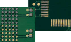
ScanINSPECT SPI provides 100% 2D non-contact verification of bridging, paste on pads, and the total area of solder paste before adding further value to the PCB.
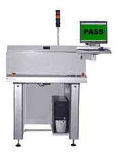
Each PCB exits the printing machine and enters ScanINSPECT SPI for 100% inspection. The part is then accepted and continues on with the process or rejected for disposition. No more surprises!
Fast & Simple Programming
ScanINSPECT SPI is quickly programmed from a golden part in a few minutes.
Increase Yield & Overall Equipment Efficiency
ScanINSPECT SPI’s powerful inspection process increases product yield by ensuring accurate solder paste printing, thus, assisting with high yields and minimal rework and/or scrap.
Missing or defective solder paste can result in lost production time and extensive rework. SPI eliminates operator fatigue and tedium from the inspection task, and automatically verifies 100% of the paste.
Missing, paste off pad, bridging, and over/under print area solder paste defects are now automatically detected. Problems are found and eliminated before value is added to defective parts.
Simplicity
ScanINSPECT SPI set up is fast and easy. In production, each board is shuttled in the system, automatically aligned and checked for defects with a PASS or FAIL inspection in seconds.
Failures are detected, logged and printed for easy analysis or rework.

Why Use ScanINSPECT SPI?
- Mandatory: 100% automatic inspection of solder paste.
- Security: Confirm solder paste on pads, total area of the paste, and detect bridging.
- Necessity: Detect errors before adding further value to defective parts.
- Flexibility: Inspect a wide variety of part sizes and shapes.
Technical Specifications*
System Specifications*
- Maximum Substrate Size: 18″ X 24″ (457mm X 610mm)
- Maximum Inspection Area: 16.5″ X 22″ (419mm X 559mm)
- Scanning Resolutions range from 200 dpi to 2400 dpi
- SMEMA Interface
- CE Certified
Footprint of Inspection Unit
- Length: 41.7″ (1060mm)
- Width: 42.9″ (1089mm)
- Height: 57″ (1450mm) excluding light tower
- Weight: 330lbs. (150kg)
Computer*
- Multi Core Processor – 3 GHz
- 1 TB 7200 RPM HD, 8 – 16 GB RAM
- CD/DVD – for archive purposes
- Flat Panel Monitor (17” or larger)
- Ethernet connection
- Windows 10 – 64-Bit
- 2 available USB ports – USB2 or USB3
*Recommended customer-supplied minimum PC requirements.
The following are trademarks of the indicated companies: Gerber, Ucamco N.V.; Windows 10, Microsoft®; ScanCAD™ and ScanINSPECT VPI™ are trademarks of ScanCAD International, Inc. *All specifications and designs subject to change without notice.*
Friendly, Flexible, Innovative & Global
ScanCAD International, Inc. continues to flourish and evolve to successfully meet ever-changing technology requirements.
All ScanCAD products were developed at the request of its customers, therefore your comments and suggestions are welcome.